Spintronics AI Completes First GaN-on-Silicon Power HEMT Wafer-Out
- Published
- Author
- Semiconductor For You
- Reads
- 516
The 650 V, 20 A GaN-on-Si device has reached wafer-level testing at CSIR-CEERI, with electrical characterisation and reliability assessment ahead.
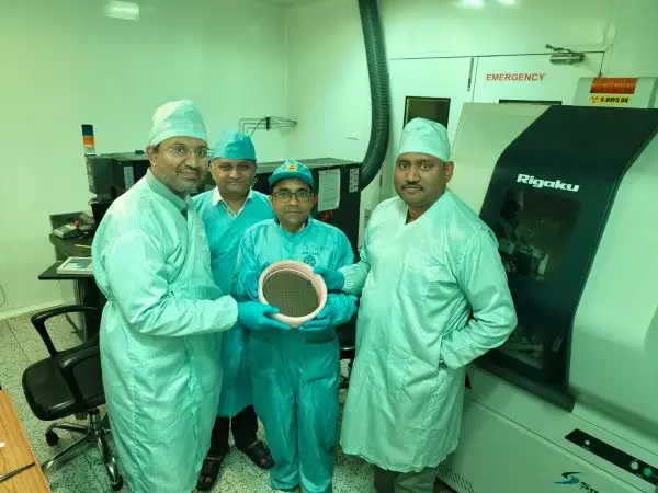
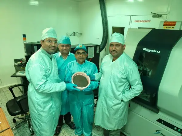
Spintronics AI Semiconductors’ GaN-on-silicon power transistor programme has produced its first fabricated wafer, moving the 650 V, 20 A device from design work into hardware evaluation. The Hyderabad-based company completed the wafer-out with CSIR-Central Electronics Engineering Research Institute (CSIR-CEERI), Pilani, and reports encouraging preliminary observations from wafer-level testing.
Wafer-out marks the end of wafer fabrication and the start of tests that examine the devices on the wafer. It is an early development milestone, rather than evidence that the transistor has met its target ratings or is ready for use in a finished product. The next results will show how the fabricated structures perform electrically and whether they can progress through reliability assessment, packaging evaluation and product qualification.
From fabricated wafer to device data
Initial wafer-level testing took place at CSIR-CEERI in Pilani under the technical guidance of Dr. Pijus Kundu, a senior scientist at the institute. Kundu described the preliminary results as encouraging and linked the work to the wider development of GaN devices for high-frequency and high-power applications. The reported observations are an initial indication from testing; no detailed electrical measurements, test conditions or device yield figures were provided.
That distinction matters for power semiconductors. A wafer can mark a successful transition from design to fabrication, while questions about switching performance, losses, stability and consistency still require measurement. Expanded electrical characterisation is planned next, followed by reliability assessment. The programme’s progress will depend on those results, and the company has not given a fixed schedule.
The target ratings are 650 V and 20 A, for a gallium nitride-on-silicon power high electron mobility transistor (HEMT). Those figures describe the intended device class; they should not be read as confirmed operating limits for the wafers now under evaluation. The development team will need to establish how the fabricated devices behave across relevant electrical conditions before product-level claims can be made.
Why GaN is being developed for power conversion
GaN is a wide-bandgap semiconductor. Compared with conventional silicon devices, GaN power HEMTs can support higher-frequency switching with lower losses, a combination that can help designers improve conversion efficiency and power density. In a power converter, faster switching can also affect the size and design of surrounding components, so the device’s characteristics matter to the complete system rather than only to the transistor itself.
Potential application areas named for the programme include electric-vehicle charging equipment, solar inverters, telecommunications and data-centre power supplies, industrial power conversion, and energy storage. These systems place different demands on voltage handling, current, switching behaviour and thermal management. The 650 V and 20 A targets give a sense of the intended power-device segment, but the eventual fit for any particular system will depend on measured performance, packaging and qualification.
For engineers selecting a power switch, a material’s theoretical advantages do not settle the design decision. The device must also perform reliably in its intended operating environment and work with the converter’s other electrical and thermal requirements. The upcoming characterisation and reliability work will therefore be more informative about practical use than the wafer-out milestone alone.
Research collaboration and development path
The work is part of a collaboration formalised through a Memorandum of Understanding between Spintronics AI and CSIR-CEERI. The institute brings more than two decades of experience in GaN devices, while Spintronics AI contributes semiconductor design, engineering and product-development capabilities. The stated aim is to advance GaN technology and carry research and design knowledge towards industry-led product development.
Spintronics AI founder and CEO Raghu Varma said the wafer-out reflects the work required to resolve design decisions before fabrication. He also credited the collaboration with CSIR-CEERI and said the company intends to demonstrate the capabilities of its engineering team through the programme. The device’s measured results will provide the next concrete evidence of how those design choices translated into fabricated hardware.
The company is also evaluating a proposed GaN semiconductor fabrication facility in Ujjain, Madhya Pradesh. The facility remains at the preliminary feasibility stage, so it is a longer-term possibility rather than part of the current device test programme. The immediate work is focused on characterisation, reliability, optimisation, packaging evaluation and qualification.
Spintronics AI managing director Srijith Paruchuri said the HEMT devices are advancing through detailed characterisation and described the wafer-out as one step in that process. He also cited progress in the company’s RF antenna and filter module development programmes. For the power device, the practical measure of progress will be the evidence emerging from electrical testing and reliability assessment. Those results will determine how closely the fabricated GaN-on-Si HEMTs approach their intended ratings and what further development is needed before they can become product candidates.