Pulsed Arc Deposition Builds Meter-Tall Titanium Single Crystals
- Published
- Author
- Aura Moreno
- Reads
- 315
A pulsed wire-arc process produced meter-tall Ti-6Al-4V single crystals and refractory-metal builds, with creep results pointing to high-temperature uses.
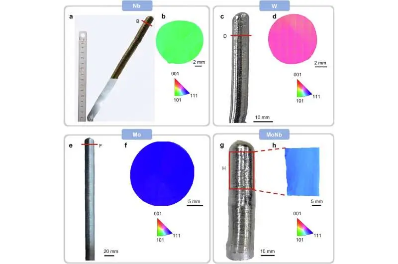
Metal additive manufacturing has produced single crystals only in limited forms; a new wire-and-arc process extends that capability to meter-tall titanium alloy rods and architected lattices. The researchers also grew single crystals of tungsten, molybdenum, niobium and a molybdenum-niobium alloy, pointing to a manufacturing route for materials that are difficult to process without grain-related defects.

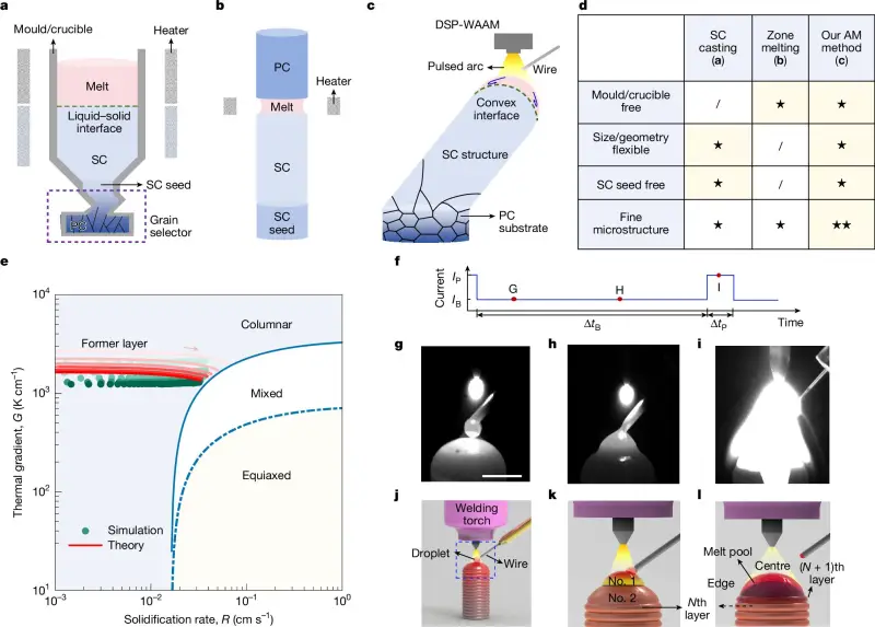
The work was carried out by researchers from Beijing Institute of Technology, Tsinghua University, Xi’an Jiaotong University and the University of California, Los Angeles. Their study, “Additive manufacturing of ultralong and architected single crystals,” describes deep-squat pulsed wire arc additive manufacturing, or DSP-WAAM. Its central idea is to control the shape of the molten region and allow a thin part of each deposited layer to remelt, so misaligned crystal growth can be corrected as the build proceeds.
Crystal growth at meter scale
The team printed Ti-6Al-4V rods about one meter tall and roughly a centimeter across, along with samples 6 mm and 20 mm in diameter. The largest sample was too wide for a complete orientation scan. Instead, the researchers mapped nine regions across its cross-section and found that they belonged to one continuous crystal.
The process also produced unsupported lattices built from zigzag struts. Each strut was a single crystal, a configuration the researchers say had not previously been produced. Their stability map links print success to both strut thickness and angle. An 8 mm strut printed at 45° under three sets of processing conditions; 13 mm and 16 mm struts did not succeed at that angle but printed correctly at 60°. That relationship gives designers a concrete constraint to consider when choosing lattice geometry.
Crystal orientation varied by less than 2° in niobium, less than 5° in tungsten and the molybdenum-niobium alloy, and less than 8° in molybdenum. Tungsten is a particularly demanding case: its hardness and brittleness, sensitivity to impurities, and steep thermal stresses make it prone to microcracking during additive manufacturing. Cracks often follow grain boundaries. Removing those boundaries through single-crystal growth could therefore help produce larger tungsten parts with fewer cracks, though the study’s results do not establish commercial performance.
The researchers found no theoretical upper limit on crystal width. In practice, increasing the part size narrows the usable range of heat input and scan speed. Those settings must keep the top of the build molten while maintaining a convex solidification front and crystal growth aligned with the desired orientation.
Why the process pulses the arc
DSP-WAAM melts wire with an electric arc whose current alternates between high and low levels. In the modeled case, the peak was 200 A and the base was 20 A. The two levels solve different problems: a steady peak current overheated the deposit until it collapsed, while a steady base current could not melt the wire.
Thermal-fluid modeling showed that pulsing produced a broad, shallow melt pool with an outward-bulging solidification front. That geometry helps suppress unwanted grains as the metal solidifies. A cross-section cut from the base of a niobium sample showed stray grains disappearing over a short distance as the single crystal took over.
Layer remelting adds another source of process tolerance. The study describes a remelting thickness of about 0.15 mm. If a region in a deposited layer does not meet the conditions for aligned crystal growth, subsequent remelting can remove it while leaving the correctly grown material intact. In effect, every layer can correct some local growth errors, supporting stable crystal formation through repeated deposition.
High-temperature performance and trade-offs
At 700°C, the printed titanium resisted creep about an order of magnitude better than predictions based on grain-size models. Creep is the gradual deformation that occurs when a material remains under load at elevated temperature. The researchers attribute the result to two features: the absence of grain boundaries and a hierarchical arrangement of alpha and beta titanium phases created during printing. Together, these features influence dislocation formation and movement, as well as the growth of voids.
Tensile testing showed that the single crystal does not lead at every temperature. Forged, polycrystalline Ti-6Al-4V had greater yield strength below about 500°C; above that point, the single crystal was stronger. Microscopy after deformation at 600°C helped explain the crossover. Boundaries in the forged material can collect dislocations and strengthen it at lower temperatures. At higher temperatures, however, those same boundaries generate many dislocations, making deformation easier.
Potential applications named by the researchers include reactor components, laser mirrors and lightweight lattices for heat shielding in extreme-temperature environments. The creep and tensile results suggest why such uses may be of interest, but practical value will depend on further validation and the requirements of each component.
A wider route to seed-free builds
Metal additive manufacturing repeatedly heats and cools deposited material, while single-crystal growth usually depends on stable thermal conditions. Earlier work had formed small single-crystal nickel alloy deposits on existing single-crystal bases, and other parts combined a single-crystal core with polycrystalline material.
Researchers in Japan previously demonstrated seed-free printing of pure single-crystal nickel using selective laser melting. They used a flat-top laser beam to create a planar melt pool, allowing crystal growth on polycrystalline stainless steel plates instead of a single-crystal build plate. Like DSP-WAAM, that method uses melt-pool shape to guide growth without a seed crystal.
The new work extends seed-free single-crystal printing from nickel to meter-tall titanium alloy builds and several refractory metals. Its most useful next measure will be whether the process can hold the required crystal orientation and mechanical performance across parts designed for demanding service.