Raspberry Pi Pico Pinout: GPIO, Power, ADC, PWM and Serial Interfaces
- Published
- Author
- peppe8o
- Reads
- 598
Pico and Pico 2 boards share a 40-pin layout, with flexible GPIO functions, analog inputs, PWM and serial buses. Key limits and model differences matter.
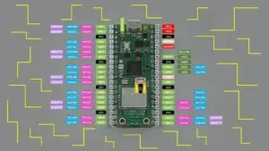
The Raspberry Pi Pico family keeps its physical connections consistent across generations, so a project built around the original Pico’s 40-pin layout can generally move to a Pico 2 without rewiring. The useful details are in the pin functions: GPIOs can serve several peripherals, some system signals aren’t exposed on the headers, and the wireless models place their debug pads differently.
This guide covers the original Pico, Pico W, Pico 2 and Pico 2 W. The RP2040 and RP2350 boards share the same 51 mm × 21 mm outline and 40 pin positions. GPIO numbering, power rails and the main SPI, I2C and UART options remain consistent. The wireless models have a different debug pad location, and the onboard LED’s connection also varies by model.
Board layout and GPIO access
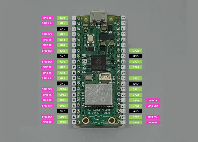
The physical pin numbers identify positions along the two 20-pin rows; GPIO names such as GP0 through GP28 identify logical signals. A pin can have more than one function, so the right connection depends on both its physical position and the peripheral configuration in software. The board’s pinout diagram is a practical reference when wiring a breadboard or checking an existing design.

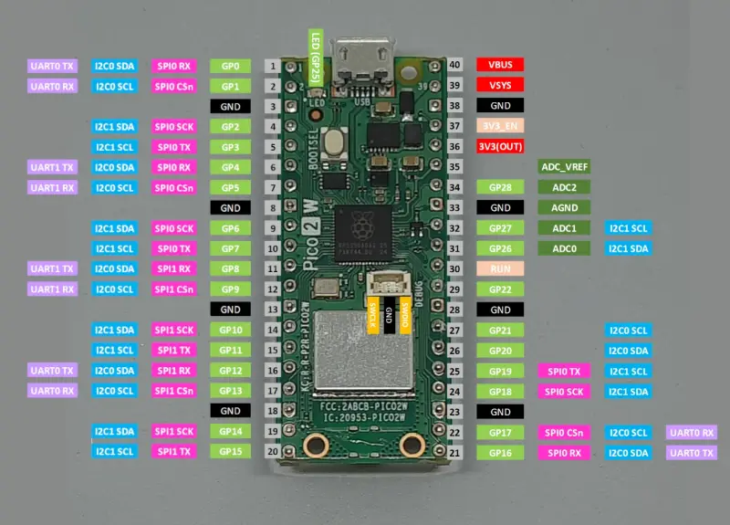
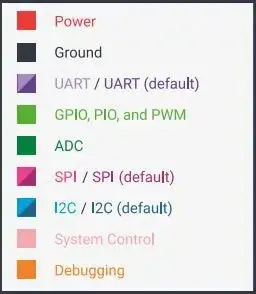
Not every GPIO number corresponds to a header pin. Several signals serve board functions internally: GP29 is ADC3 and measures VSYS divided by three; GP24 senses whether VBUS is present; and GP23 controls the onboard switched-mode power supply’s power-save pin. The board also provides eight physical ground connections, distributed across the header.
The onboard LED is another model-specific detail. On the original Pico, it is connected to GP25. On Pico W and Pico 2 W, the LED uses a different connection; MicroPython exposes it through the name LED. Code or wiring assumptions that target GP25 should therefore be checked before moving between wireless and non-wireless boards.

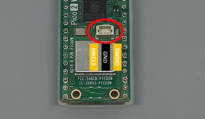
Wireless models place the SWD debug pads near the wireless module, between it and the main microcontroller. On Pico and Pico 2 without wireless, the pads sit along the board’s bottom edge. The pinout illustrations show these locations and identify the other signal groups.
Some boards are sold without header pins soldered in place. They need two 20-pin strips added before they can plug into a breadboard or accept jumper wires. The soldering process requires care around the hot iron; the MagPi guide to soldering Pico GPIO headers covers that job.

Power rails and current limits
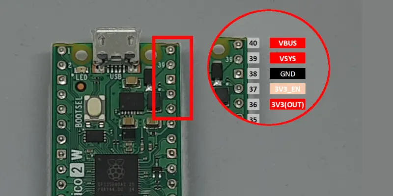
The power pins sit at one end of the header and serve different roles. VBUS is the USB supply input, nominally 5 V when a powered USB connection is present and 0 V when it isn’t. VSYS is the main system input, with an allowed range of 1.8 V to 5.5 V; the onboard switched-mode supply uses it to produce the board’s 3.3 V rail.
| Signal | Physical pin | Function and stated characteristics |
|---|---|---|
| VBUS | 40 | USB input voltage; nominally 5 V from a powered USB supply. |
| VSYS | 39 | Main supply input, allowed range 1.8 V to 5.5 V. |
| 3V3_EN | 37 | Enables the onboard supply and is pulled up to VSYS through a 100 kΩ resistor. Pulling it low disables the 3.3 V rails and powers down the Pico chip. |
| 3V3 (OUT) | 36 | Onboard supply output for the processor and I/O. External load should remain below 300 mA. |
| GND | 3, 8, 13, 18, 23, 28, 33, 38 | Eight physical ground connections. |
GPIO current limits need similar attention. The maximum total IOVDD current is the combined current sourced by all GPIOs. The figures given for the wireless Pico 2 W with RP2350 and Pico W with RP2040 are 100 mA and 50 mA, respectively. A conservative per-pin guideline is to keep sourced current at or below 10 mA. These figures describe different limits: staying within a per-pin guideline does not by itself guarantee that the combined GPIO load is acceptable.

Analog inputs and reference voltage
The RP2040 and RP2350 include an ADC, giving the Pico family analog inputs for sensors and other variable voltage signals. The board uses its regulated 3.3 V rail as the ADC reference by default rather than a separate onboard reference chip. An external reference can be supplied at ADC_VREF when a more stable reference is needed.
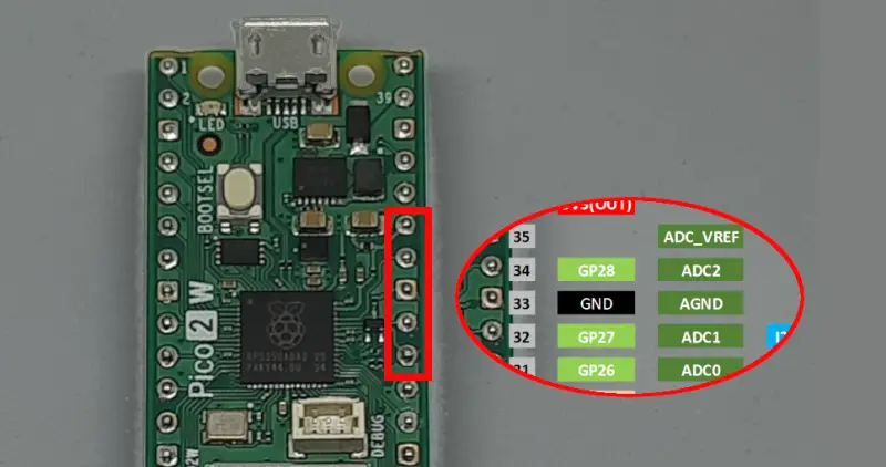
| Signal | Physical pin | Function |
|---|---|---|
| ADC0 | 31 (GP26) | Analog channel 0; also available as GPIO26 or I2C1 SDA. |
| ADC1 | 32 (GP27) | Analog channel 1; also available as GPIO27 or I2C1 SCL. |
| ADC2 | 34 (GP28) | Analog channel 2; also available as GPIO28. |
| ADC_VREF | 35 | Input for an external analog reference voltage. |
| AGND | 33 (GND) | Analog ground reference for the ADC input group. |
The ADC is described as a 12-bit successive-approximation converter, mapping the range between AGND and ADC_VREF into 4,096 levels, numbered 0 to 4095. A further ADC channel, ADC3 on GP29, is internal rather than available on a header. It measures VSYS/3, allowing software to monitor the system supply.

PWM output mapping
The Pico series has eight PWM blocks, each with A and B outputs. The source describes up to 16 controllable PWM outputs, with PWM-capable functions available across the GPIOs. Multiple physical pins can map to the same PWM channel; configuring a channel can therefore produce the same signal on its corresponding mapped pins.
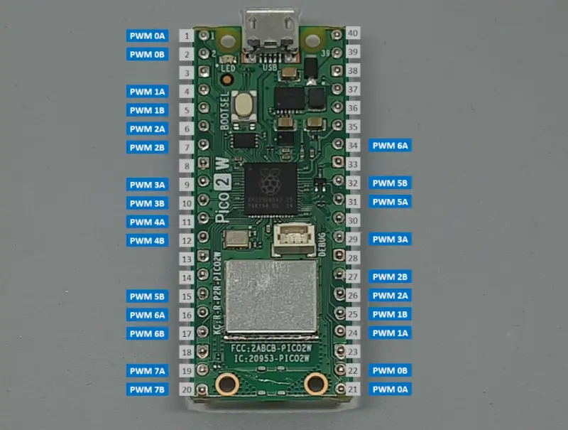
| PWM block | GPIO options | Physical pin numbers |
|---|---|---|
| PWM 0A / 0B | GP0, GP1, GP16, GP17 | 1, 2, 21, 22 |
| PWM 1A / 1B | GP2, GP3, GP18, GP19 | 4, 5, 24, 25 |
| PWM 2A / 2B | GP4, GP5, GP20, GP21 | 6, 7, 26, 27 |
| PWM 3A / 3B | GP6, GP7, GP22, GP23* | 9, 10, 29 |
| PWM 4A / 4B | GP8, GP9, GP24* | 11, 12 |
| PWM 5A / 5B | GP10, GP11, GP25 (LED) | 14, 15, 1 on Pico; internal on Pico W and Pico 2 W |
| PWM 6A / 6B | GP12, GP13, GP26 | 16, 17, 31 |
| PWM 7A / 7B | GP14, GP15, GP27, GP28 | 19, 20, 32, 34 |
*GP23, GP24 and GP25 have board-level roles, including power-save control, VBUS sensing and the onboard LED, depending on the model. Their peripheral mapping should be considered alongside those built-in functions.

UART, I2C and SPI
Both the RP2040 and RP2350 provide two UART, two I2C and two SPI peripherals. The functions can be assigned to several GPIO groups, giving a design some flexibility when other pins are already committed. The options below list the mappings in the source pinout.
UART
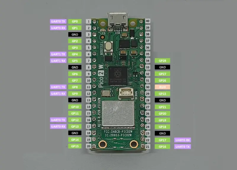
UART provides an asynchronous serial transmit and receive connection. UART0 has TX on GP0, physical pin 1, and RX on GP1, pin 2; alternatives are GP12/GP13 on pins 16/17 and GP16/GP17 on pins 21/22. UART1 uses GP4/GP5 on pins 6/7, with GP8/GP9 on pins 11/12 as an alternative pair.

I2C
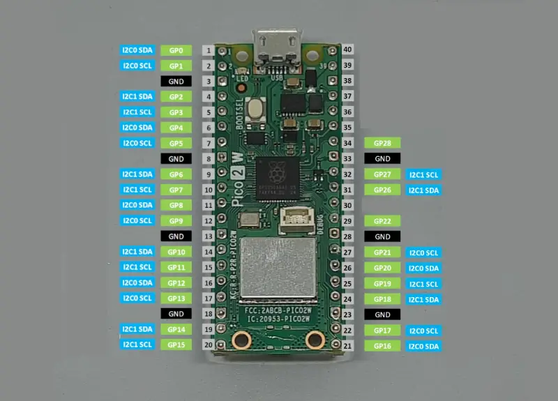
I2C is a synchronous two-wire bus using SDA for data and SCL for the clock. I2C0 pairs GP4 with GP5 on pins 6/7, or GP16 with GP17 on pins 21/22. The listed alternatives include GP0, GP8, GP12, GP20 and GP24. I2C1 pairs GP2 with GP3 on pins 4/5, or GP10 with GP11 on pins 14/15; its listed alternatives include GP6, GP14, GP18, GP26 and GP27.
SPI
SPI uses clock, transmit, receive and chip-select signals for synchronous communication. The listed SPI0 group on GP16–GP19 assigns RX to GP16, CSn to GP17, SCK to GP18 and TX to GP19, on physical pins 21, 22, 24 and 25. Alternative SPI0 groups are GP0–GP3 on pins 1, 2, 4 and 5, and GP4–GP7 on pins 6, 7, 9 and 10.
SPI1’s primary group is GP8–GP11 on pins 11, 12, 14 and 15, in RX, CSn, SCK and TX order. Its alternative group uses GP12–GP15 on pins 16, 17, 19 and 20.
SWD debugging and a rail check
The three-pin Serial Wire Debug connection consists of SWDIO, GND and SWCLK. An external debugger can use it to reset the board, flash firmware and debug code without relying on the BOOTSEL button. Its location depends on the board: Pico and Pico 2 place the pads at the bottom edge, while Pico W and Pico 2 W place them centrally near the wireless hardware.
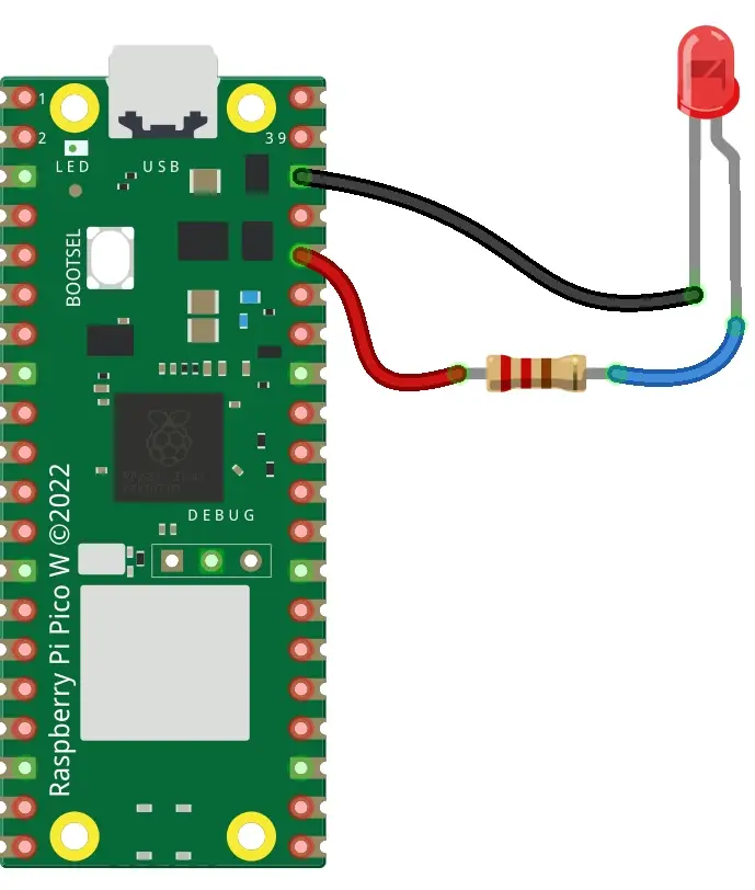
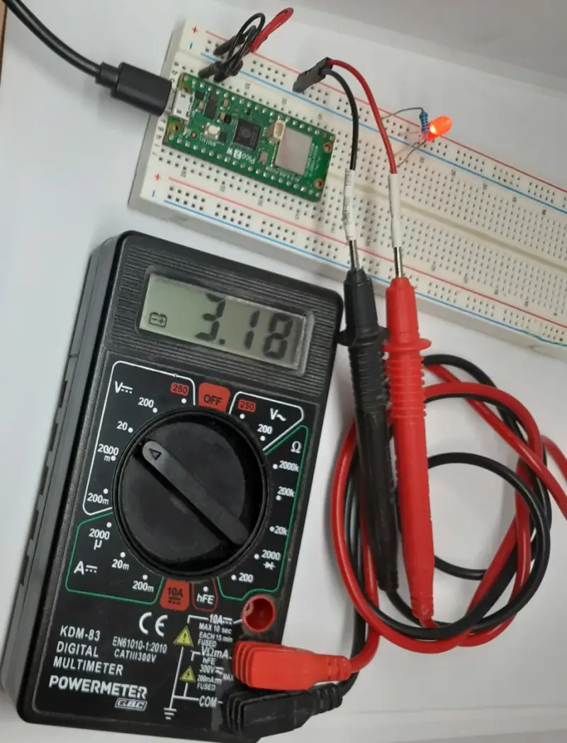
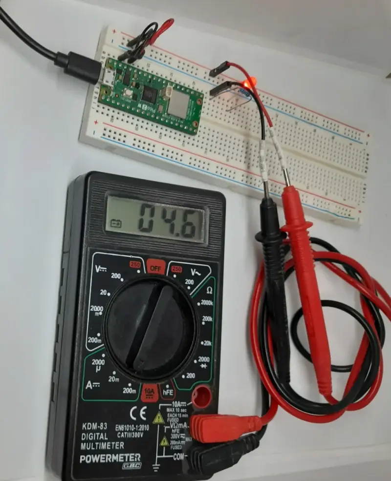
A simple LED load illustrates how to check the 3V3 output. The described circuit connects physical pin 36 (3V3 OUT) through a 220 Ω or 330 Ω resistor to an LED’s anode, then connects its cathode to pin 38 (GND). The resistor limits current through the LED.
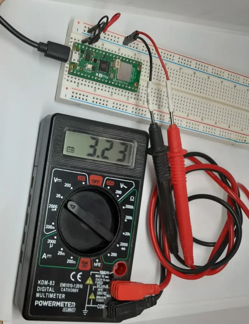
In a reported bench measurement, the unloaded rail measured 3.23 V. With the LED lit, the measured value was 3.18 V, a drop of 0.05 V. Those readings describe one setup, rather than a guaranteed output for every board or load. The test also proposes measuring LED current with a multimeter inserted in series between the resistor and 3V3 output; the measured load should be considered against the power and GPIO limits relevant to the chosen connection.
The Pico family’s consistent 40-pin layout makes board replacement and enclosure reuse straightforward at the physical level. For a working design, the details to verify are the selected GPIO function, the model-specific LED and debug connections, and the current budget of the supply and I/O.